Image
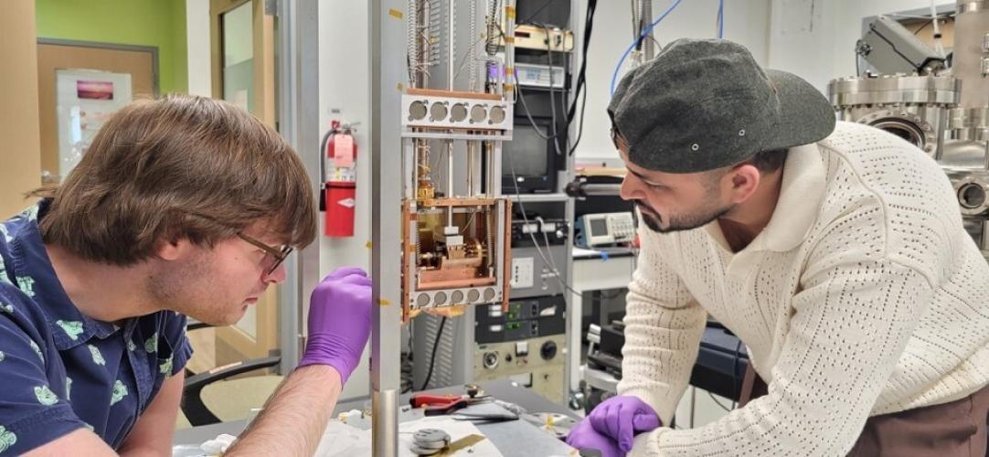
In a laboratory at Ohio University, a microscope unlike any you'd find in a catalog is constructed to quietly image the surfaces of exotic magnetic materials, one atom at a time.
The instrument, a variable-temperature scanning tunneling microscope (VT-STM), was designed and constructed from the ground up by Ali Abbas (recently graduated) and Nick Goman, doctoral candidates in experimental condensed matter physics working in the lab of Dr Arthur R. Smith at the Nanoscale and Quantum Phenomena Institute (NQPI) in OHIO’s Physics and Astronomy Department.
Scanning tunneling microscopes work on a principle of quantum mechanics called tunneling. When an atomically sharp metal tip is brought within a nanometer of a surface, electrons “tunnel” across the gap, producing a tiny electrical current that is exquisitely sensitive to distance. By scanning the tip across a sample and tracking that current, researchers can map surfaces with atomic resolution, resolving features roughly a million times smaller than the width of a human hair.
While commercial STMs can cost hundreds of thousands of dollars, the NQPI instrument was built in-house, following the rugged “Pan-style” design widely used in low-temperature research. The microscope operates in ultra-high vacuum and can cool samples to below 30 Kelvin, or roughly minus 400 degrees Fahrenheit. Reaching those conditions is essential for studying quantum and Kagome materials, whose most interesting electronic and magnetic behaviors often emerge only at cryogenic temperatures.
Every stage of the project, from the mechanical design of the microscope head and vibration isolation, to the wiring, coarse-approach mechanics, was carried out at Ohio University. The copper braids for cryogenic cooling needed special fabrication and were fabricated at SVT Associates. A manuscript describing the instrument's design and performance is in preparation for the journal Review of Scientific Instruments.
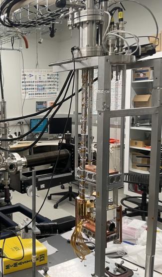
The microscope is being installed and is currently baking. Abbas’ doctoral research focuses on thin films of manganese gallium nitride (Mn₃GaN), an “antiperovskite” magnetic material whose manganese atoms form a kagome lattice, a woven, star-like geometric pattern named after a traditional Japanese basket weave. Materials with this structure host unusual forms of magnetism and electronic transport that make them candidates for future low-power memory and spintronic technologies. The films are grown in the same laboratory using molecular beam epitaxy, a technique for depositing crystalline layers with atomic precision, and the new STM allows the team to examine their surfaces directly.
The project also reflects NQPI's emphasis on hands-on graduate training. Abbas secured the NQPI fellowship last year to finish the construction of VT-STM. Building a research-grade cryogenic instrument from scratch demands expertise in ultra-high-vacuum technology, electronics wirings, and low-temperature physics, a combination of skills in high demand in both academia and industry.
That training is already paying off: Abbas recently accepted a position as a research engineer at the National High Magnetic Field Laboratory (NHMFL) in Tallahassee, Florida, the world's largest and highest-powered magnet laboratory, where he will join the DC Field facility.
This research has been supported by the U.S. Department of Energy, Office of Basic Energy Sciences, Division of Materials Sciences and Engineering.